Locations
Company type
Result types
Industries
Employees
Founding year
The B2B platform for the best purchasing descision. Identify and compare relevant B2B manufacturers, suppliers and retailers
Close
Filter
Result configuration
Continents
Select continent
Locations
Result types
Company type
Select company type
Industries
Select industry
Company status
Select company status preset
Number of employees
Min.
Max.
Founding year
EULITHA AG
Kirchdorf (BE), Switzerland
A
11-50 Employees
2006
Key takeaway
Eulitha specializes in innovative nano-lithography technologies that enhance the performance and efficiency of photonic devices. As a leader in high-quality lithography solutions for photonics manufacturing, Eulitha supports customers throughout all stages of productization.
Reference
Core business
Lithography for photonics - EULITHA
Teledyne DALSA Bromont
Bromont, Canada
A
251-500 Employees
2002
Key takeaway
Teledyne MEMS specializes in advanced micro-machining solutions, including photolithography, for various MEMS applications in sectors like automotive and medical. With over three decades of experience, they provide the necessary scalability and quality control to support the development of innovative BioMEMS products.
Reference
Service
Photolithography | Teledyne MEMS
Eulitha
Kirchdorf (BE), Switzerland
A
1-10 Employees
2006
Key takeaway
Eulitha specializes in innovative nano-lithography technologies that enhance the performance and efficiency of photonic devices, making it a key player in high-quality lithography solutions for photonics manufacturing.
Reference
Core business
Eulitha
Lithography for Photonics. Eulitha provides nanolithography services and equipment for research and production.
Looking for more accurate results?
Find the right companies for free by entering your custom query!
25M+ companies
250M+ products
Free to use
MSG Lithoglas
Dresden, Germany
A
11-50 Employees
2010
Key takeaway
Lithoglas specializes in designing and manufacturing high-quality wafer-level components using advanced semiconductor and MEMS processing technologies, making it a key player in the field. Their patented technologies, particularly Lithoglas® Windows for DUV applications, enhance light output and thermal performance, which is crucial for applications involving UV LEDs and sensors.
Reference
Core business
MSG Lithoglas GmbH
Lithographics Inc.
Nashville, United States
B
51-100 Employees
1975
Key takeaway
Lithographics is a multi-service printing and graphics company that has been part of the Nashville business community since 1975. They offer a wide range of printing solutions and have expertise in printed communications, serving various industries.
Reference
Core business
Lithographics Leadership - Lithographics
SUSS MicroTec
Garching bei München, Germany
A
501-1000 Employees
1949
Key takeaway
The SUSS MicroTec Group is a prominent supplier of equipment and process solutions for microstructuring applications, highlighting its expertise in backend lithography and photomask processing, which are crucial for semiconductor manufacturing.
Reference
Product
Semiconductor Manufacturing Technologies | SUSS MicroTec
Atomica Corp. (formerly IMT)
Santa Barbara, United States
B
101-250 Employees
2000
Key takeaway
Atomica specializes in advanced lithography technologies, including state-of-the-art photolithography and innovative greyscale (3D) lithography, which are integral to their comprehensive wafer fabrication services.
Reference
Service
MEMS Photolithography and Greyscale Lithography | Atomica

Masimo Semiconductor, Inc.
Hudson, United States
B
11-50 Employees
2012
Key takeaway
Masimo Semiconductor specializes in the development and manufacturing of III-V opto-electronic devices, utilizing advanced photolithography and other fabrication techniques. Their extensive experience and capabilities in custom device fabrication and production make them a reliable partner for semiconductor solutions.
Reference
Product
Foundry Services - Masimo Semiconductor
Fabrication, Development & Production Masimo Semiconductor operates a complete compound semiconductor device fabrication line focused on the fabrication of custom devices, as well as development, prototyping, pilot production and manufacturing. Capabilities of the custom and production wafer processing laboratory at Masimo Semiconductor range from prototype development to full production and include CAD design of photolithographic …
Hightec MC AG
Lenzburg, Switzerland
A
11-50 Employees
1992
Key takeaway
Hightec MC AG is a specialized microelectronics manufacturer that focuses on the development and production of high-quality custom-made products using thin film technology, including photolithography. Their innovative HiCoFlex® solution highlights their expertise in creating ultra-thin flexible multilayer printed circuits, which is relevant to semiconductor lithography.
Reference
Service
Photolithography – Hightec MC AG
S-Cubed
Montville Township, United States
B
11-50 Employees
1994
Key takeaway
S-Cubed specializes in semiconductor lithography, offering innovative equipment designed with a modular architecture that allows for tailored solutions to meet specific throughput and processing needs. Their commitment to reliability and functionality in a compact design positions them as a key player in the lithography equipment market.
Reference
Core business
lithography-treatment - S-Cubed Semiconductor Lithography Equipment Manufacturer
Technologies which have been searched by others and may be interesting for you:
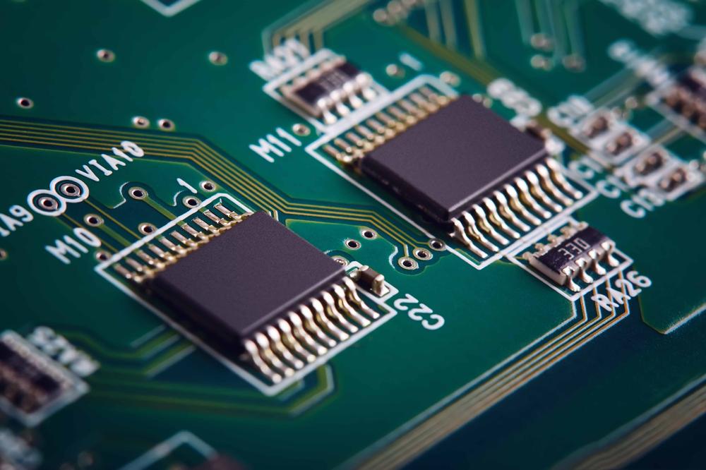
Lithography in the semiconductor industry is a critical process used to transfer patterns onto a silicon wafer. This technique involves using light to project intricate designs onto a photosensitive material, allowing for the creation of integrated circuits. Advanced lithography techniques, such as extreme ultraviolet (EUV) lithography, enable the production of smaller and more powerful semiconductor devices by achieving finer resolutions. The performance and precision of lithography equipment directly impact the capabilities of semiconductor manufacturers. As technology progresses, providers of lithography semiconductor solutions continuously innovate to meet the demands for increased speed, efficiency, and miniaturization in chip production.
Lithography in semiconductor technology is a critical process used to transfer patterns onto semiconductor wafers. This technique involves the application of light to a photosensitive material known as photoresist. Initially, a mask with specific patterns is placed over the wafer coated with photoresist. When exposed to light, the photoresist undergoes a chemical change, allowing selective etching or deposition of materials in the desired areas. After exposure, the wafer is developed, washing away either the exposed or unexposed photoresist, depending on whether a positive or negative photoresist is used. This results in a precise pattern on the wafer. Subsequent steps include etching the exposed areas of the wafer and depositing additional materials, leading to the formation of integrated circuits. The accuracy and resolution of lithography are essential for producing smaller and more efficient semiconductor devices, enabling advancements in technology.
Recent advancements in lithography semiconductor technology focus on pushing the boundaries of miniaturization and efficiency. Extreme Ultraviolet (EUV) Lithography has emerged as a groundbreaking technique, enabling the production of smaller transistors with higher performance. This technology utilizes shorter wavelengths of light to achieve finer resolutions, which is crucial for manufacturing next-generation chips. Additionally, multi-patterning techniques have been developed to further enhance resolution without requiring new equipment. These techniques allow manufacturers to create complex patterns on silicon wafers, significantly improving chip density. Innovations in computational lithography also play a vital role, utilizing sophisticated algorithms to optimize patterning processes, thereby enhancing yield and reducing defects during manufacturing. These advancements collectively drive the semiconductor industry towards more powerful and efficient electronic devices.
Lithography semiconductors play a crucial role in chip manufacturing as they are essential for defining patterns on silicon wafers. This process involves transferring intricate designs onto the wafer surface, which ultimately determines the functionality and performance of the microchips. The precision of lithography directly impacts the size and efficiency of transistors and other components within the chip. With advancements in lithography technology, manufacturers can achieve smaller feature sizes, leading to more powerful and energy-efficient chips. As a result, lithography is fundamental in driving innovation and meeting the increasing demand for high-performance electronics in various applications.
The lithography semiconductor industry encounters several significant challenges. One major issue is the rapid pace of technological advancement, which demands constant innovation and adaptation. As semiconductor devices become smaller and more complex, lithography techniques must evolve to meet these new requirements, often leading to increased costs and development time. Another challenge lies in the high capital expenditure associated with advanced lithography equipment. The cost of acquiring and maintaining state-of-the-art machines can be prohibitive for many providers. Additionally, supply chain disruptions and the global semiconductor shortage have further complicated procurement and production processes. These factors collectively create a demanding environment for lithography semiconductor providers.
Some interesting numbers and facts about your company results for Lithography Semiconductor
| Country with most fitting companies | United States |
| Amount of fitting manufacturers | 9672 |
| Amount of suitable service providers | 6788 |
| Average amount of employees | 11-50 |
| Oldest suiting company | 1949 |
| Youngest suiting company | 2012 |
20%
40%
60%
80%
Some interesting questions that has been asked about the results you have just received for Lithography Semiconductor
What are related technologies to Lithography Semiconductor?
Based on our calculations related technologies to Lithography Semiconductor are Magnets, Printed Electronics, Industrial Amplifiers, Electronic Transducers, Electronic Oscillators
Which industries are mostly working on Lithography Semiconductor?
The most represented industries which are working in Lithography Semiconductor are Other, Electronics and Electrical engineering, IT, Software and Services, Semiconductor, Printing
How does ensun find these Lithography Semiconductor Companies?
ensun uses an advanced search and ranking system capable of sifting through millions of companies and hundreds of millions of products and services to identify suitable matches. This is achieved by leveraging cutting-edge technologies, including Artificial Intelligence.