Home - GETec Microscopy
We are a multidisciplinary team consisting of specialists in the fields of physics, electrical and mechanical engineering, biological sciences, semiconductor and MEMS processing, business and finance. We are more than happy to announce that Jürgen Schlütter joins GETec Microscopy as our new CEO. GETec was founded in 2011 as GETec KG and has been transferred to GETec Microscopy GmbH as its full legal successor in Oct. GETec Microscopy offers innovative Atomic Force Microscopy solutions for seamless integration into existing host systems like Scanning Electron Microscopes. In partnership with our customers, we develop dedicated nano analysis tools based on pre-engineered modules. It’s open access design allows to simultaneously operate SEM and AFM inside the SEM vacuum chamber. GETec’s leading Atomic Force Microscopy in SEM technology nicely complements Quantum Design’s strong position in materials property characterization instrumentation and optics,” stated Jerry Daviess, Chief Executive Officer for Quantum Design International. Especially the possibility to immediately control the result of your nanofabrication experiment is a real benefit!”.
Verified
Correlative in-situ analysis of bone collagen - GETec Microscopy
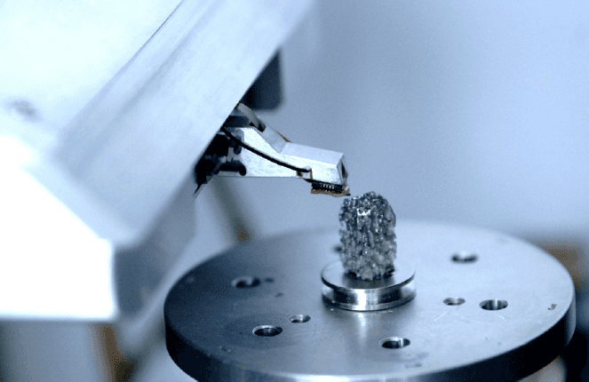
Fast and easy identification and imaging of lacunae with AFSEM™: Real 3D topography with sub-nm resolution
Verified
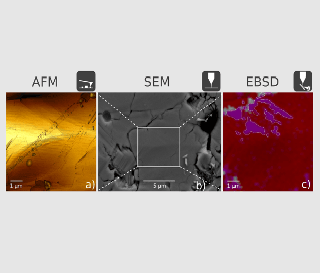
Correlative EBSD, SEM and AFM analysis of ZrO2 ceramics - GETec Microscopy
In situ analysis of martensitic transition in ZrO2 ceramics with AFSEM®
Verified
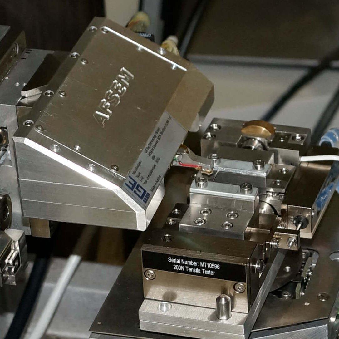
Analysis of tensile stress samples with AFSEM® - GETec Microscopy
Observe the sample changes by SEM, measure details with AFSEM®
View all products
Keywords
Industries
2019, Feb.: 1st AFSEM® application video - GETec Microscopy
Have you seen our first AFSEM® application video? In it we analyse a specific bone structure, called lacunae, and show you how this experiment benefits from the unique properties of AFSEM®.
Where is GETec Microscopy located?
The company GETec Microscopy is located in Vienna, Austria. It's worth noting that the company may has more corporate locations
How many employees does GETec Microscopy approximately have?
As of the latest available information GETec Microscopy has around 11-50 employees worldwide.
In which industries does GETec Microscopy mainly work?
The company GETec Microscopy has it's main focus in the industries of Science and Engineering

EB Tec GmbH
Germany
1-10 Employees
2013
Quantum Design Microscopy
Germany
1-10 Employees
Neaspec
Germany
2007
SG Technologies Ltd
United Kingdom
51-100 Employees
1940
GEC Gräber Engineering Consultants GmbH
Germany
1-10 Employees
2005
Spacetek
Switzerland
1-10 Employees
2018
EDAX, Inc.
United States
101-250 Employees
1962
GEC Instruments
United States
Topics which have been searched by others and may be interesting for you: